|
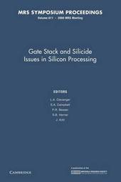
Gate Stack and Silicide Issues in Silicon Processing: Volume 611
Paperback / softback
Main Details
| Title |
Gate Stack and Silicide Issues in Silicon Processing: Volume 611
|
| Authors and Contributors |
Edited by L. A. Clevenger
|
|
Edited by S. A. Campbell
|
|
Edited by P. R. Besser
|
|
Edited by S. B. Herner
|
|
Edited by J. Kittl
|
| Series | MRS Proceedings |
|---|
| Physical Properties |
| Format:Paperback / softback | | Pages:254 | | Dimensions(mm): Height 229,Width 152 |
|
| Category/Genre | Materials science |
|---|
| ISBN/Barcode |
9781107413160
|
| Classifications | Dewey:620.193 |
|---|
| Audience | | Postgraduate, Research & Scholarly | | Professional & Vocational | |
|---|
|
Publishing Details |
| Publisher |
Cambridge University Press
|
| Imprint |
Cambridge University Press
|
| Publication Date |
5 June 2014 |
| Publication Country |
United Kingdom
|
Description
As the feature size of microelectronic devices approaches the deep submicron regime, the process development and integration issues related to gate stack and silicide processing are key challenges. Gate leakage is rising due to direct tunneling. Power and reliability concerns are expected to limit the ultimate scaling of SiO2-based insulators to about 1.5nm. Gate insulators must not deleteriously affect the interface quality, thermal stability, charge trapping, or process integration. Metal gate materials and damascene gates are being investigated, in conjunction with the application of a high-permittivity gate insulator, to provide sufficient device performance at ULSI dimensions. The silicidation process is also coming under pressure. Narrow device widths and decreasing junction depths are making the formation of low-leakage, low-resistance silicide straps extremely difficult. Producing shallower junctions via ion implantation is inhibited by transient enhanced diffusion and low beam currents at low implantation energies. Gate stack and contact film effects, such as point defect injection, extended defect formation, and stress on ultrashallow junction formation must be considered.
|